- 您现在的位置:买卖IC网 > Sheet目录1994 > DS3911T+ (Maxim Integrated Products)IC DAC 10BIT I2C QUAD 14TDFN
DS3911
Temperature-Controlled, Nonvolatile,
I2C Quad DAC
16
Maxim Integrated
Register Description
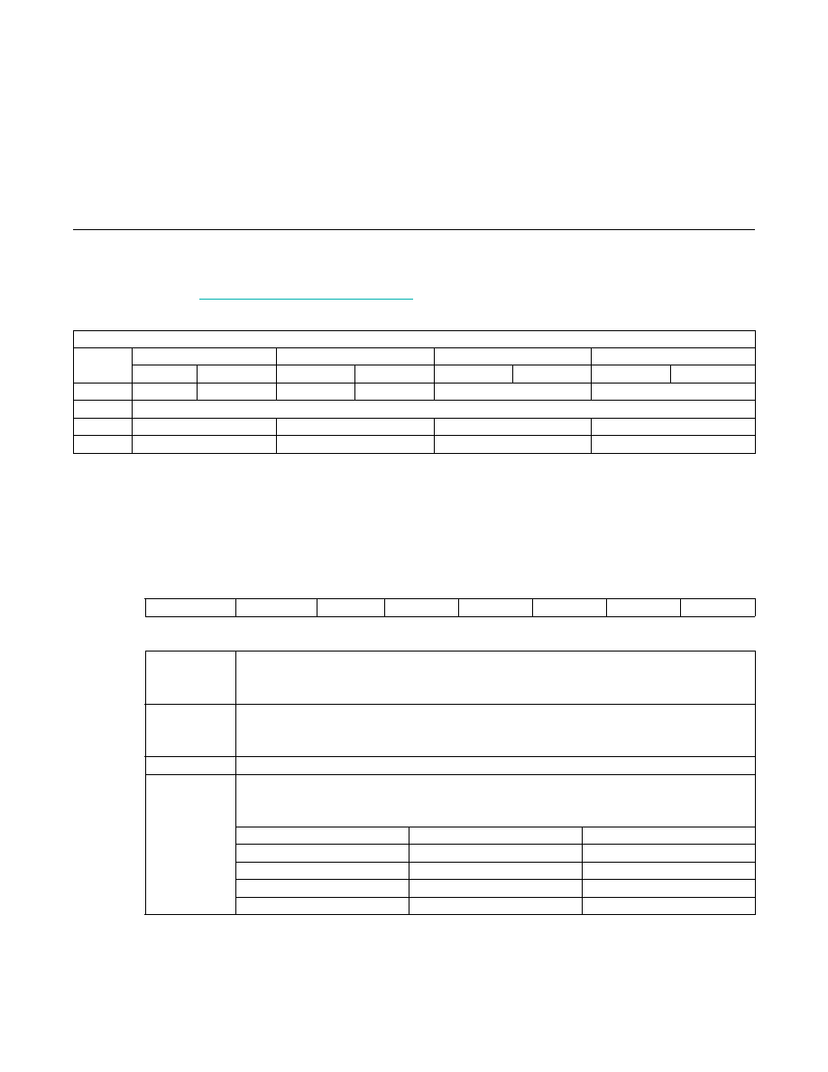
This register map shows each byte/word (2-byte) in terms of its row and byte/word placement in the memory. The first
byte in the row is located in memory at the row address (hexadecimal) in the leftmost column. Each subsequent byte/
word on the row is one/two memory locations beyond the previous byte/word’s address. A total of 8 bytes are present
on each row. See the Lower Memory Register Descriptions section for more information about each of these bytes.
Lower Memory Register Map
Lower Memory Register Descriptions
Lower Memory, Register 00h: CTRL
LOWER MEMORY
ADDR
(HEX)
WORD 0
WORD 1
WORD 2
WORD 3
BYTE 0
BYTE 1
BYTE 2
BYTE 3
BYTE 4
BYTE 5
BYTE 6
BYTE 7
00h
CTRL
MODE
SRAM
TINDEX
TEMP VALUE
VCC VALUE
08h
—
10h
DAC3 VALUE
DAC2 VALUE
DAC1 VALUE
DAC0 VALUE
78h
DAC3 POR
DAC2 POR
DAC1 POR
DAC0 POR
POWER-ON VALUE
00h
ACCESS
R/W
MEMORY TYPE
Volatile
00h
DONETEMP
DONEVCC
SRAM
TS3
TS2
TS1
TS0
BIT 7
BIT 0
BIT 7
DONETEMP: Done Temp Status
0 = Temperature conversion in progress.
1 = Temperature conversion completed since this bit was last cleared.
BIT 6
DONEVCC: Done VCC Status
0 = VCC conversion in progress.
1 = VCC conversion completed since this bit was last cleared.
BITS 5:4
SRAM: General-Purpose SRAM. These bits have no affect on device operation.
BITS 3:0
TS[3:0]: Table Select. The device’s memory tables are accessed by writing the desired table
value in this bit field. The device only contains four addressable memory tables, 04h–07h, and
therefore the values listed below are the only usable options.
TS[3:0]
TABLE SELECTED
CORRESPONDING DAC LUT
0100b
04h
0
0101b
05h
1
0110b
06h
2
0111b
07h
3
发布紧急采购,3分钟左右您将得到回复。
相关PDF资料
DS4000KI/WBGA
IC OSC TCXO 19.44MHZ 24-BGA
DS4026S+WCN
IC OSC TCXO 25MHZ 16-SOIC
DS4100HW+
IC OSC CLOCK 100MHZ 10LCCC
DS4266P+
IC OSC CLOCK 266MHZ 10-LCCC
DS4302Z-020/T&R
IC DAC 5-BIT SGL 0-2.0V 8-SOIC
DS4302Z-020+
IC DAC 5-BIT SGL 0-2.0V 8-SOIC
DS4311P+
IC OSC CLOCK 311.04MHZ 10-LCCC
DS4404N+
IC DAC 4CH I2C ADJ 14-TDFN
相关代理商/技术参数
DS3911T+T
功能描述:ADC / DAC多通道 Fast APD Bias RoHS:否 制造商:Texas Instruments 转换速率: 分辨率:8 bit 接口类型:SPI 电压参考: 电源电压-最大:3.6 V 电源电压-最小:2 V 最大工作温度:+ 85 C 安装风格:SMD/SMT 封装 / 箱体:VQFN-40
DS3920
制造商:MAXIM 制造商全称:Maxim Integrated Products 功能描述:Fast Current Mirror
DS3920_1112
制造商:MAXIM 制造商全称:Maxim Integrated Products 功能描述:Fast Current Mirror
DS3920T-001+
功能描述:电流和电力监控器、调节器 Fast APD Bias
RoHS:否 制造商:STMicroelectronics 产品:Current Regulators 电源电压-最大:48 V 电源电压-最小:5.5 V 工作温度范围:- 40 C to + 150 C 安装风格:SMD/SMT 封装 / 箱体:HPSO-8 封装:Reel
DS3920T-001+T
功能描述:电流和电力监控器、调节器 Fast APD Bias w/20mA limit
RoHS:否 制造商:STMicroelectronics 产品:Current Regulators 电源电压-最大:48 V 电源电压-最小:5.5 V 工作温度范围:- 40 C to + 150 C 安装风格:SMD/SMT 封装 / 箱体:HPSO-8 封装:Reel
DS3920T-002+
功能描述:电流和电力监控器、调节器 Fast Current Mirror
RoHS:否 制造商:STMicroelectronics 产品:Current Regulators 电源电压-最大:48 V 电源电压-最小:5.5 V 工作温度范围:- 40 C to + 150 C 安装风格:SMD/SMT 封装 / 箱体:HPSO-8 封装:Reel
DS3920T-002+T
功能描述:电流和电力监控器、调节器 Fast APD Bias w/20mA limit
RoHS:否 制造商:STMicroelectronics 产品:Current Regulators 电源电压-最大:48 V 电源电压-最小:5.5 V 工作温度范围:- 40 C to + 150 C 安装风格:SMD/SMT 封装 / 箱体:HPSO-8 封装:Reel
DS3922T+
制造商:Maxim Integrated Products 功能描述:ADV APD MIRROR W/INT FET & STAT OUT - Rail/Tube 制造商:Maxim Integrated Products 功能描述:IC CURRENT MIRROR TQFN
